In electronics, some components quietly do most of the heavy lifting without getting much attention. The diode is one of them. From converting AC to DC in power supplies to protecting sensitive circuits, emitting light, sensing light, and even generating laser beams, diodes are everywhere.
For an engineering student, understanding diodes is non-negotiable. They appear in basic circuit theory, analog electronics, power electronics, digital systems, communication circuits, and embedded systems.
This tutorial builds a solid conceptual foundation—starting from what a diode is, how it is built, how it behaves electrically, and where it is used in real life.
What Is a Diode?
A diode is a two-terminal device that conducts electric current primarily in one direction and blocks it in the opposite direction. In simple words, a diode is an electrical one-way valve.
The semiconductor diode is formed by simply bringing n and p-type materials together (constructed from the same base, Ge or Si). That’s why it is also called a pn junction diode or crystal diode.
The two terminals of a diode are:
- Anode (A)
- Cathode (K)
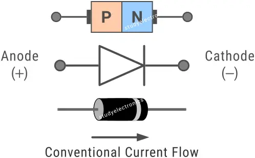
A standard diode symbol is given as above. The arrowhead is the cathode and represents the direction of the conventional current flow. In a real diode, this side is marked with a white band.
When the anode is at a higher potential than the cathode, the diode conducts current. And when the polarity is reversed, the diode ideally blocks current.
Physical Structure of a Diode
A diode is constructed by joining two differently doped semiconductor materials. Usually, a P-type semiconductor and an N-type semiconductor. That’s why it is also called a PN Junction diode.
A P-type semiconductor has holes as majority carriers and electrons as minority carriers, while an N-type semiconductor has electrons as majority carriers and holes as minority carriers.
When P-type and N-type materials are joined, electrons from the N-side diffuse into the P-side, and holes from the P-side diffuse into the N-side. This creates a region near the junction that is depleted of mobile charge carriers, called the depletion region.
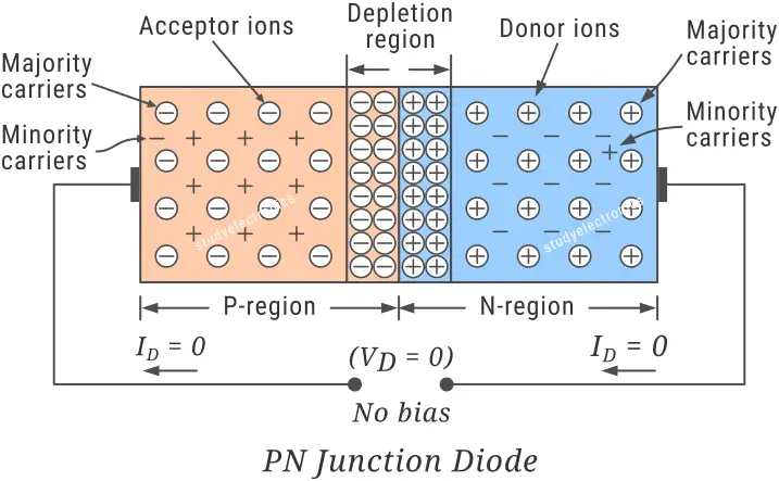
The depletion region contains fixed ions, which create an internal electric field. This field opposes further diffusion. The resulting voltage is called the barrier potential. It is approximately 0.7 V for silicon and 0.3 V for germanium. This barrier must be overcome for the diode to conduct electricity.
Characteristics of a Diode
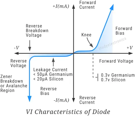
The behavior of a diode is best understood by its V–I (Voltage–Current) characteristics. The V-I characteristic of a typical PN junction diode is given below.
To fully understand diode behavior, its V–I characteristics are analyzed under three different biasing conditions.
Applying an external voltage across a diode to control its operation is called biasing. There are three biasing conditions: no bias, forward bias, and reverse bias.
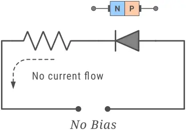
Zero Bias or No Bias
When no external voltage is applied to the terminal of a diode, it is said to be in the no-bias condition. In the no-bias condition, the net current flow is zero.
Forward Bias Characteristics
A diode is forward-biased when the anode is connected to the positive terminal and the cathode is connected to the negative terminal of a voltage source.
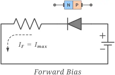
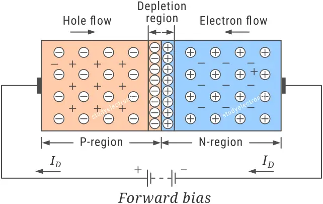
In forward bias, the applied external voltage opposes the internal electric field of the depletion region. The majority carriers (electrons in the N-type region and holes in the P-type region) are pushed toward the junction. As a result, the depletion region narrows, the potential barrier decreases, and the diode conducts current.
In the image below, you can see the internal structure of a PN junction under forward bias conditions.
In the graph below, you can see that in forward bias, the current increases very slowly when the applied voltage is below the barrier potential. After crossing the barrier potential, the current increases rapidly.
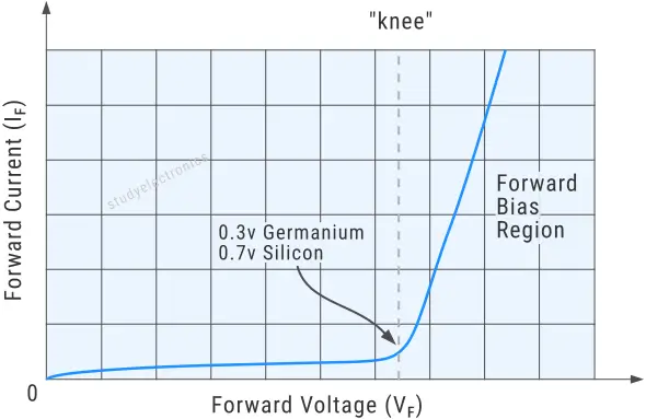
In the forward-bias V–I curve, the initial region is called the cut-in (or threshold) region, where the diode current is almost negligible. For silicon diodes, this threshold is approximately 0.7 V.
After crossing the cut-in (threshold) voltage, the current increases rapidly with a small increase in voltage. This is called the forward bias region, which represents the normal conducting operation of the diode.
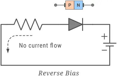
Reverse Bias Characteristics
A diode is reverse-biased when the anode is connected to the negative terminal and the cathode is connected to the positive terminal of a voltage source.
In reverse bias, the anode is connected to the negative terminal and the cathode to the positive terminal. The applied external voltage adds to the internal electric field of the depletion region. As a result, the majority carriers are pulled away from the junction—electrons in the N-type move toward the positive terminal, and holes in the P-type move toward the negative terminal.
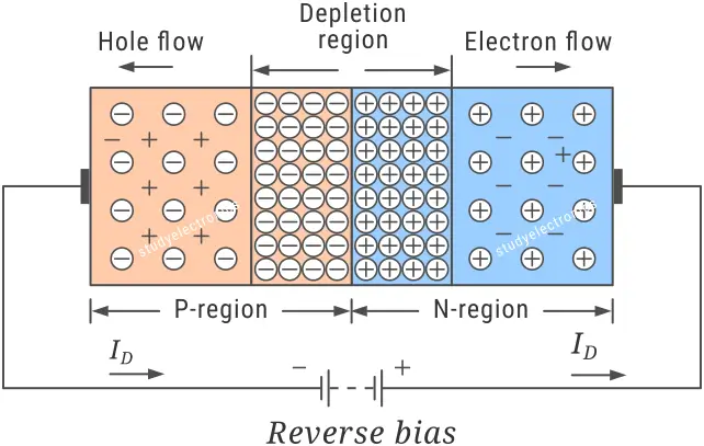
When these charge carriers move away, more fixed ions remain uncovered near the junction. This increases the width of the space-charge region, so the depletion region widens under reverse bias. This wider potential barrier blocks current flow, and only a very small leakage current flows due to minority carriers.
In the graph below, you can observe that in reverse bias, the diode initially allows only a very small leakage current due to minority carriers. This current remains nearly constant as the reverse voltage increases.
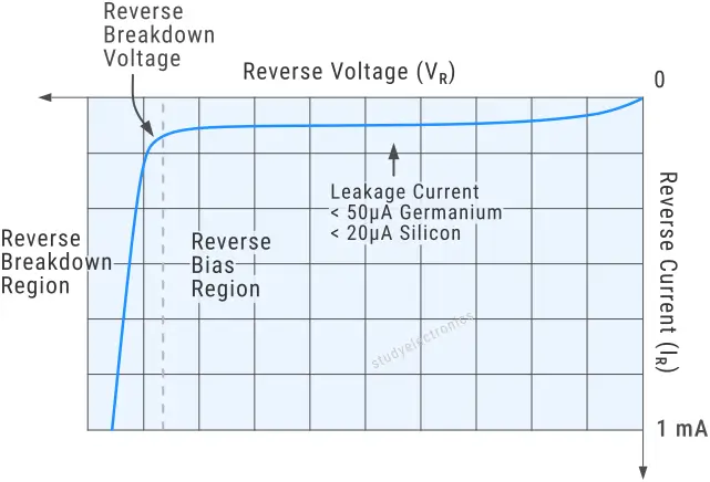
However, if the reverse voltage exceeds a certain critical value, the diode conducts heavily. This condition is called reverse breakdown, and the corresponding voltage is known as the breakdown voltage. Beyond this point, the diode must be protected by a current-limiting resistor (unless it is specifically designed for breakdown operation, such as a Zener diode) to prevent damage.
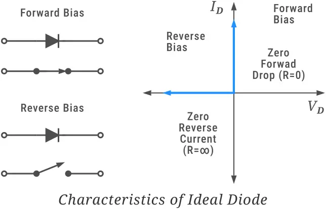
Ideal Diode vs Practical Diode
In theory, a diode conducts perfectly in forward bias and completely blocks current in reverse bias. However, in practical applications, it does not behave exactly like this. An ideal diode is a theoretical model. In forward bias, it has zero voltage drop and zero resistance, allowing current to flow freely. In reverse bias, it has infinite resistance and completely blocks current, with no leakage.
A practical diode, on the other hand, has non-ideal characteristics. It requires a threshold voltage (about 0.7 V for silicon) before conducting, and it has a small forward resistance. In reverse bias, a small leakage current flows, and if the reverse voltage exceeds the breakdown voltage, it may conduct heavily.
Diode Laws
A diode does not behave linearly with respect to the applied voltage. The current through a diode increases rapidly after a certain voltage, showing a nonlinear and exponential behavior. Because of this, we cannot analyze a diode accurately using a basic linear equation.
To describe this nonlinear behavior mathematically, we use the diode law (also known as the Shockley diode equation). It provides a relationship between the voltage across the diode and the current flowing through it, which is essential for proper circuit analysis and design.
The DC current-voltage characteristics of an ideal PN junction diode are described by the Shockley diode equation.
Where,
- ID is the diode current.
- IS is the reverse saturation current.
- VD is the DC voltage across the diode.
- n is the identity factor.
- VT is the thermal voltage.
From the above equation, we can also derive the diode resistance.
Types of Diodes
Different types of diodes are developed for specific applications, and they all follow the basic principles of diodes but differ slightly from the common PN junction diode that you saw above.
Some of the most important types are:
- PN Junction Diode
- Zener Diode
- Schotty Diode
- Light Emitting Diode (LED)
- Photodiode
- Varactor Diode
- Tunnel Diode
PN Junction Diode
It is the most common type of diode. It is used in rectification, signal detection, switching applications, and general-purpose electronic circuits.
All the characteristics and construction discussed above refer to the PN junction diode.
Zener Diodes
A Zener diode is a specially designed PN junction diode that is intended to operate in the reverse breakdown region. Unlike a normal diode, it can safely conduct current when the reverse voltage exceeds a specified value called the Zener voltage, without getting damaged.
The key feature of a Zener diode is its ability to maintain a constant output voltage over a wide range of current. This makes it highly reliable for voltage regulation and protection. Zener diodes are commonly used as voltage regulators, voltage references, and overvoltage protection devices in power supplies and electronic circuits.
Schottky Diode
A Schottky diode is a special type of diode formed by a metal–semiconductor junction instead of a PN junction. It switches very fast because it does not depend on minority carriers. It has a low forward voltage drop (typically 0.2–0.3 V), which results in lower power loss.
They are widely used in high-speed switching circuits, switch-mode power supplies (SMPS), RF applications, and as freewheeling diodes in power electronics.
Light Emitting Diode (LED)
A Light Emitting Diode (LED) is a PN junction diode that emits light when forward-biased. The light is produced due to electron–hole recombination in the semiconductor material. LEDs are highly energy efficient, have a long lifespan, and are available in different colors depending on the semiconductor material used.
LEDs are commonly used in indicators, displays, lighting systems, optical communication, and status signaling in electronic circuits.
Photodiode
A Photodiode is a light-sensitive PN junction diode that converts light energy into electrical current. It is usually operated in reverse bias.
The reverse current of a photodiode increases proportionally with the intensity of incident light, making it fast and highly sensitive to light. Photodiodes are widely used in light sensors, optical communication systems, IR receivers, camera sensors, and automatic light control circuits.
Varactor Diode
A Varactor diode (or varicap diode) is a PN junction diode designed to operate in reverse bias, where it behaves like a voltage-controlled capacitor. The junction capacitance of a varactor diode changes with the applied reverse voltage, allowing electronic tuning without mechanical components.
Varactor diodes are commonly used in RF tuning circuits, voltage-controlled oscillators (VCOs), phase-locked loops (PLLs), FM radios, and frequency modulators.
Tunnel Diode
A Tunnel diode is a heavily doped PN junction diode that exhibits the quantum tunneling effect. It has a unique negative resistance region in its V–I characteristics, which allows very fast operation at low voltages.
Tunnel diodes are used in high-frequency oscillators, microwave circuits, fast switching applications, and low-power amplifiers.