In the previous article, you learned about the centre-tapped full-wave rectifier, but it works only with a centre-tap transformer. It makes the design bulkier and inconvenient in many applications. The bridge rectifier solves this limitation by using four diodes, which allows full-wave rectification without the need for a centre-tapped transformer.
In this article, you will learn about full-wave bridge rectifier. By the end of this tutorial, you will understand the bridge rectifier circuit, its working principle, output waveform, and the important formulas used to analyze its performance.
What is a Bridge Rectifier?
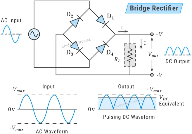
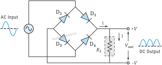
A bridge rectifier is a type of full-wave rectifier that uses four diodes arranged in a bridge configuration to convert an AC (Alternating Current) input into a DC (Direct Current) output. It rectifies both the positive and negative half-cycles of the AC signal and produces a pulsing DC output.
The four diodes are connected in such a way that two diodes conduct during the positive half-cycle of the AC input and the other two conduct during the negative half-cycle. As a result, the load always receives current in the same direction.
The bridge rectifier does not require a centre-tapped transformer. Instead, it operates with a normal transformer with a single secondary winding. This reduces the overall circuit size. Because of this advantage, the bridge rectifier is one of the most commonly used rectifier circuits in power supply systems.
Bridge Rectifier Circuit
The bridge rectifier circuit consists of four diodes (D₁, D₂, D₃, and D₄) connected in a bridge arrangement. The AC voltage source is connected across one diagonal of the bridge, and the load resistor is connected across the other diagonal, where the rectified DC output appears.
Each diode in the circuit is placed in such a way that current can flow through the load in the same direction regardless of the polarity of the AC input. The AC source continuously alternates between positive and negative half-cycles, but the diode arrangement ensures that the load current never changes direction.
Working of a Bridge Rectifier
When the AC input is applied to the circuit, only two diodes conduct during a particular half cycle, while the other two remain reverse-biased and block current. During the next half cycle, the conducting pair of diodes changes, but the direction of current through the load remains the same.
During the positive half-cycle of the AC input, the upper terminal of the AC source becomes positive, and the lower terminal becomes negative. In this condition, diodes D₁ and D₃ become forward biased, while diodes D₂ and D₄ become reverse biased.
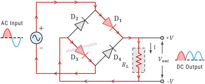
Current flows from the positive terminal of the AC source through diode D₁, then through the load resistor, and finally returns to the source through diode D₃. Because of this, the current flows through the load resistor in a specific direction. As a result, a positive voltage appears across the load.
The output waveform corresponding to this half cycle follows the shape of the positive half of the input waveform.
During the negative half-cycle of the AC input, the polarity of the AC source reverses. The upper terminal becomes negative, and the lower terminal becomes positive.
In this case, diodes D₂ and D₄ become forward biased, while diodes D1 and D3 become reverse biased. Current flows from the positive terminal of the AC source through diode D4, then through the load resistor, and returns through diode D2.
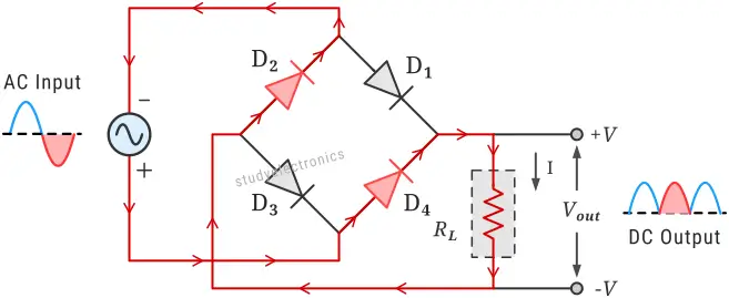
Although the input polarity has reversed, the direction of current through the load resistor remains the same as in the positive half-cycle. So again, a positive output pulse appears across the load.
The output waveform corresponding to this half cycle is the inverted form of the negative half of the input waveform.
So you can see that both halves of the AC waveform contribute to the output voltage. The positive half of the waveform passes through the circuit, while the negative half-cycle is inverted by the diode arrangement and produces a full-wave rectified DC signal.
Bridge Rectifier Output Waveform
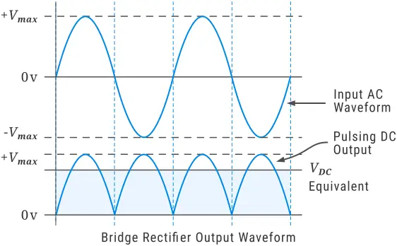
From the above waveform diagram, you can see that both the positive and negative parts of the AC signal appear in the output. The positive half remains the same, while the negative half is inverted. As a result, the output voltage across the load is always positive.
The output waveform is a pulsing DC signal with a frequency that is twice the frequency of the input AC signal. For example, if the input AC frequency is 50 Hz, the rectified output frequency becomes 100 Hz.
The output is not a pure DC signal, but it is much smoother than the output of a half-wave rectifier. However, the waveform still contains a noticeable amount of ripple. In practical power supplies, these ripples are reduced by using filter circuits such as capacitors, inductors, or RC filters.
Bridge Rectifier with Smoothing Capacitor
The ripple present in the output can be reduced in many ways. One of the simplest and most commonly used methods is to use a capacitor.
The circuit remains the same as seen previously; only a capacitor is added across the load resistor. The larger the capacitor size, the less the ripple in the output voltage, but it also increases the cost and size of the circuit.
In practical power supplies, the capacitor value usually ranges between 100 µF and several thousand microfarads, depending on the load current and the required level of smoothing.
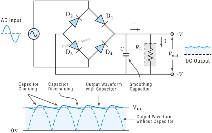
During each output pulse, when the voltage rises from low to high, the capacitor charges and stores energy. When the voltage falls from the peak, the capacitor discharges slowly and maintains the output supply.
For a bridge rectifier with a capacitor filter, the ripple factor is approximately given by
where
= frequency of the AC supply
= load resistance
= capacitance of the filter capacitor
This formula shows that the ripple factor decreases when the capacitance increases.
Formula
Several mathematical formulas are used to analyze the performance of a bridge rectifier. These formulas help determine how effectively the circuit converts AC power into DC power and how much ripple is present in the output.
Some of the important parameters of a bridge rectifier, such as DC output voltage, RMS value, form factor, peak factor, and rectification efficiency, are discussed below.
DC Output Voltage
DC output voltage is the average value of the rectified voltage across the load resistor in a rectifier circuit. It indicates the effective DC level produced by the rectifier.
For an ideal full-wave bridge rectifier, the average DC output voltage is given bywhere is the maximum (peak) value of the input AC voltage.
This formula shows that the DC output voltage depends on the peak value of the input AC signal. In practical circuits, the actual DC output voltage is slightly lower because two diodes conduct in series during each half-cycle, which introduces a small voltage drop across the diodes.
RMS Value
The RMS (Root Mean Square) value represents the effective value of the rectified output voltage. It is equivalent to the DC voltage that would produce the same power in a resistive load.
For a full-wave rectified waveform, the RMS voltage is given byThe RMS value indicates the equivalent DC voltage that would produce the same power dissipation in the load resistor.
Ripple Factor
Ripple Factor is a measure of the amount of ripple present in the rectifier output. It is defined as the ratio of the RMS value of the AC component to the DC component of the output voltage.
Mathematically,
For a full-wave bridge rectifier, the ripple factor is:
where
Vrms is the RMS value of the total output voltage, and
VDC is the average DC output voltage.
Substituting the RMS and DC values into the equation, we obtain γ = 0.482. This indicates significantly less ripple than a half-wave rectifier.
Form Factor
The form factor is defined as the ratio of the RMS value of the output voltage to its average DC value.
For an ideal full-wave rectifier, the form factor is approximately
This parameter indicates how much the waveform deviates from pure DC. A value close to 1 indicates a smoother waveform.
Peak Factor
The peak factor (also known as crest factor) is the ratio of the peak value of the output voltage to its RMS value.For a full-wave rectified waveform, the peak factor is approximately
This parameter indicates how high the waveform peaks are relative to their effective value.
Rectification Efficiency
The rectification efficiency measures how effectively the rectifier converts AC input power into DC output power.
For an ideal full-wave bridge rectifier, the maximum rectification efficiency is approximately
This means that about 81.2% of the AC input power is converted into useful DC output power, while the remaining power is lost mainly in the diodes and other circuit components.
Peak Inverse Voltage
Peak Inverse Voltage (PIV) is the maximum reverse voltage that a diode can safely handle without breaking down.
In a bridge rectifier, each diode must withstand a peak inverse voltage equal to the maximum value of the input AC voltage. Therefore, for a bridge rectifier,
where is the peak value of the input AC voltage.
This means that the diode used in the circuit must have a PIV rating greater than the peak input voltage to ensure safe operation. If the PIV rating of the diode is lower than the applied reverse voltage, the diode may fail, and the rectifier circuit will stop working properly.